Preferred embodiment describes in detail
First embodiment
Fig. 1 is the schematic circuit diagram according to the sequence type optical-electrical converter of first embodiment of the invention.The sequence type optical-electrical converter refers to a kind of like this optical-electrical converter, and it is used for implementing resetting of electric charge and optical charge is stored in the output of each photodiode of the imageing sensor that is connected in parallel to each other, mobile simultaneously sequential.
Opto-electronic conversion piece An shows the opto-electronic conversion piece of n position.The quantity of opto-electronic conversion piece is identical with the quantity of pixel, and the opto-electronic conversion piece is connected in global semaphore line 11 by corresponding channel selector switch 7.Whole being configured among Fig. 7 of optical-electrical converter is illustrated.
The circuit of this embodiment comprises: as the photodiode 1 of photoelectric conversion unit; Reset switch 2 as reset unit; Amplifying unit 3; Transmission switch 4 as the charge transfer unit; Capacitor 5; Constitute the MOS transistor 6 of MOS source follower; Channel selector switch 7 as the channel selecting unit; Global semaphore line 11; And first current source 8.
Amplifying unit 3 can be made of MOS source follower, voltage follower amplifier etc., and also can be provided with amplifier and enable terminal 10, and mode of operation is selected by it.In addition, parasitic capacitance 9 is present between the grid and source of MOS transistor 6.
Fig. 2 is a sequential chart, and it is corresponding to the schematic circuit diagram according to the sequence type optical-electrical converter of first embodiment of the invention.
When according to Φ R (n) reset switch 2 being become ON, the voltage that appears at the lead-out terminal Vdi place of photodiode 1 is fixed in reference voltage V reset.On the other hand, when according to Φ R (n) reset switch 2 being become OFF, the voltage that appears at lead-out terminal Vdi place is got one by adding the value that obtains to reference voltage V reset by noise.Becoming random noise by noise is because electromotive force becomes unstable, and no matter when reset.Therefore, occur, only be necessary to obtain poor between the output voltage that the output voltage of amplifier 3 after resetting and photodiode accumulate amplifier 3 after the optical charge subsequently in order to prevent random noise.
Like this, as shown in Figure 2, after reset switch 2 being become OFF according to Φ R (n), transmit switch 4 according to Φ T1 (n) thus being become ON reads into electric capacity 5 with time interval TR with reference signal.Reference signal is held one-period in electric capacity 5.In this time interval, optical charge is accumulated in the photodiode 1, and appears at the electromotive force at lead-out terminal Vdi place and the amount of optical charge fluctuates accordingly.When the Φ SCH (n) according to following one-period became channel selector switch 7 into ON, the reference signal that is maintained in the electric capacity 5 was read out global semaphore line 11 with time interval REF.Next, if Φ T1 (n) thus being become ON will read into capacitor 5 corresponding to the light signal of the quantity of electric charge of accumulation in photodiode 1 with time interval TS, then this light signal is read out global semaphore line 11.Become ON if Φ is T1 (n), then light signal is accumulated in capacitor 5.Yet, if in Φ T1 (n) is maintained at the time interval TS of ON state, the drivability of amplifying unit 3 is configured to obtain appear at the solution (settling) of the electromotive force at terminal V1 place, and then Φ SCH (n) time interval of being maintained at the ON state can be shortened to allow to realize high speed operation.
According to above-described operation, if obtained poor between the output voltage VO UT on the global semaphore line 11 in the time interval SIG of output voltage VO UT on the global semaphore line 11 in the time interval REF of Φ SCH (n) and Φ SCH (n), then might remove the random noise and the fixed pattern noise that cause by reset switch 2.
After Φ T1 (n) was become OFF, Φ SCH (n) was become OFF, and Φ R (n) is become ON to carry out photodiode 1 ensuing resetting.Then, Φ T1 (n) thus being become ON once more reads into capacitor 5 with time interval TR with reference signal.
By after being become OFF, the channel selector switch 7 of next bit is become the operation of ON with the reference signal that begins to read next bit according to Φ SCH (n+1) at Φ SCH (n).Other pulse of all of n+1 position is maintained at the time interval of ON state from the mobile backward Φ SCH of the pulse of n position.The scope that is used to store the time interval of each light-receiving element is become the time point that the time point of OFF is finished up to the time interval TS of the Φ of following one-period T1 (n) from Φ R (n).Like this, this time interval also will be moved according to the position.
Light signal that has been read out and the difference between the reference signal are obtained in correlated double sample circuit etc.For example, this process can use the circuit of the piece C of the prior art example shown in Figure 16 to realize.
Second embodiment
Fig. 3 is the schematic circuit diagram according to the sequence type optical-electrical converter of second embodiment of the invention.With the difference in the configuration of Fig. 1 be the source that second current source 51 is linked in MOS transistor 6.Second current source 51 is designed to become ON and OFF according to enable signal Φ RR, and when second current source 51 is maintained at the ON state, and identical with first current source 8 basically electric current is caught to flow by second current source 51.
Fig. 5 is a sequential chart, and it is corresponding to the schematic circuit diagram according to the sequence type optical-electrical converter of second embodiment of the invention.
When according to Φ R (n) reset switch 2 being become ON, the voltage that appears at the lead-out terminal Vdi place of photodiode 1 is fixed in reference voltage V reset.On the other hand, when according to Φ R (n) reset switch 2 being become OFF, the voltage that appears at lead-out terminal Vdi place is got one by adding the value that obtains to reference voltage V reset by noise.Becoming random noise by noise is because electromotive force becomes unstable, and no matter when reset.Therefore, occur, only be necessary to obtain poor between the output voltage that the output voltage of amplifier 3 after resetting and photodiode accumulate amplifier 3 after the optical charge subsequently in order to prevent random noise.
Like this, as shown in Figure 5, after reset switch 2 being become OFF according to Φ R (n), transmit switch 4 according to Φ T1 (n) thus being become ON reads into electric capacity 5 with time interval TR with reference signal.At this moment, second current source 51 is become ON according to enable signal Φ RR (n).Reference signal is held one-period in electric capacity 5.In this time interval, optical charge is accumulated in the photodiode 1, and appears at the electromotive force at lead-out terminal Vdi place and the amount of optical charge fluctuates accordingly.When the Φ SCH (n) according to following one-period became channel selector switch 7 into ON, the reference signal that is maintained in the electric capacity 5 was read out global semaphore line 11 with time interval REF.Next, become ON light signal is read into capacitor 5 if Φ is T1 (n), then this light signal is read out global semaphore line 11.
At this moment, first current source 8 is become ON, and second current source 51 is become OFF.First current source 8 and second current source 51 are designed to make substantially the same ON electric current therefrom to flow through.Like this, when reference signal being read into capacitor 23 with time interval R1, appear at the electromotive force at the source electrode place of MOS transistor 6 can be basically identical with when light signal being read into capacitor 23 with time interval S1.Therefore might reduce the influence that 9 pairs of quilts of parasitic capacitance accumulate the electric charge in capacitor 5, this makes the deviation of dark output voltage diminish.
According to above-described operation, if obtained poor between the output voltage VO UT on the global semaphore line 11 in the time interval SIG of output voltage VO UT on the global semaphore line 11 in the time interval REF of Φ SCH (n) and Φ SCH (n), then might remove the random noise and the fixed pattern noise that cause by reset switch 2.Next, by after being become OFF, Φ SCH (n) is become OFF and Φ R (n) and is become ON photodiode is ensuing to be resetted to carry out at Φ T1 (n).Then, Φ T1 (n) thus being become ON once more reads into capacitor 5 with time interval TR with reference signal.
By after being become OFF, the channel selector switch 7 of next bit is become the operation of ON with the reference signal that begins to read next bit according to Φ SCH (n+1) at Φ SCH (n).Other pulse of all of n+1 position is maintained at the time interval of ON state from the mobile backward Φ SCH of the pulse of n position.
Difference between light signal and the reference signal is obtained in correlated double sample circuit etc.For example, this process can use the circuit of the piece C of the prior art example shown in Figure 16 to realize.
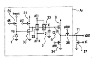
Fig. 4 is the circuit diagram according to the sequence type optical-electrical converter of second embodiment of the invention.Reset switch 2 shown in Fig. 1, amplifying unit 3, transmission switch 4, second current source 51, channel selector switch 7 and first current source 8 are replaced to MOS switch 35, MOS source follower 30 and current source 31, transmission gate 32 and pseudo-switch (dummy switch) 33, MOS current source 34, MOS switch 36 and MOS current source 37 respectively.Note,, then become in configuration identical with sequence type optical-electrical converter according to first embodiment according to the sequence type optical-electrical converter of present embodiment if MOS current source 34 is removed.
Fig. 6 is a sequential chart, and it is corresponding to the circuit diagram according to the sequence type optical-electrical converter of second embodiment of the invention.With the difference of Fig. 5 be that Φ I1 is used rather than Φ SEL.In addition, although do not illustrate in Fig. 6, Φ T1X is the inversion signal of Φ T1.
In the circuit of Fig. 4, amplifier 30 becomes ON and OFF controls according to the gate voltage of current source 31.That is to say, when Φ T1 equals supply voltage on level, do not have electric current to be caught to flow and therefore amplifier 30 be maintained at the OFF state, and when signal Phi T1 has than the low appropriate voltage of supply voltage, electric current be caught to flow and therefore amplifier 30 be maintained at the ON state.
Because in the circuit of Fig. 2, the source electromotive force of substrate potential and MOS source follower 30 is public, can make gain near 1.
In addition, when reference signal REF is read out, appears at terminal V1 place and comprise being read out of Φ T1 by the electromotive force of noise.Yet, when light signal SIG is read out, appears at terminal V1 place and do not comprise being read out of Φ T1 by the electromotive force of noise.For this reason, Φ T1's becomes dark output bias by noise component(s).In order to reduce dark output bias, transmission gate 32 rather than transmission switch 4 are used, and pseudo-switch 33 also is provided.The nmos pass transistor of transmission gate and PMOS transistor equate each other dimensionally, and the nmos pass transistor of pseudo-switch 33 and PMOS transistor are half of size of the gate region of transmission gate transistor.
When enable signal Φ RR equaled the GND electromotive force on level, MOS current source 34 was maintained at the OFF state, and when enable signal Φ RR had suitable electromotive force, MOS current source 34 was maintained at the ON state.The electromotive force that is in the enable signal Φ RR of ON state is designed to make the electrorheological that flows by MOS current source 34 must be substantially equal to the electric current that flows by MOS current source 37.For seeking to simplify, when the size of MOS current source 34 is appropriately determin, also can make the electromotive force of the enable signal Φ RR that is in the ON state equal supply voltage.Above-mentioned situation is MOS transistor 6, MOS current source 34 and MOS current source 37 each particular case that all are made of NMOS.Yet they also can be made of PMOS.
The 3rd embodiment
Fig. 8 is the schematic circuit diagram according to the batch-type optical-electrical converter of third embodiment of the invention.The batch-type optical-electrical converter refers to a kind of like this optical-electrical converter, and it is used for implementing resetting of electric charge and will be connected in parallel to each other and with the optical charge of the output of each photodiode of identical sequential memory image transducer.Opto-electronic conversion piece An shows the opto-electronic conversion piece of n position.The quantity of opto-electronic conversion piece is identical with the quantity of pixel, and the opto-electronic conversion piece is connected in global semaphore line 11 by corresponding channel selector switch 7.Whole being configured among Fig. 7 of optical-electrical converter is illustrated.
The circuit of this embodiment comprises: as the photodiode 1 of photoelectric conversion unit; Each all is used as the transmission switch 18,19 and 20 of charge transfer unit; Reset switch 2 as reset unit; Amplifying unit 15,16 and 17; Capacitor 21,22 and 23; Formation MOS gets in the source MOS transistor 6 with device; Channel selector switch 7 as the channel selecting unit; Global semaphore line 11; And first current source 8. Amplifying unit 15,16 and 17 each all can constitute by MOS source follower, voltage follower amplifier etc., and also can be provided amplifier respectively and enable terminal 12,12 and 14 and be used for the selection operation state.In addition, parasitic capacitance 9 is present between the grid and source of MOS transistor 6.
Figure 10 is a sequential chart, and it is corresponding to the schematic circuit diagram according to the batch-type optical-electrical converter of third embodiment of the invention.Φ R, Φ T1 and Φ SEL1 are all bit manipulations simultaneously.The time interval of the Φ SEL2 that the time interval S1 of the Φ T2 that light signal is transmitted and light signal are transmitted also is used for all positions simultaneously.The time interval of the Φ SEL2 that the time interval R1 of the Φ T2 that reference signal is transmitted, reference signal are transmitted and other pulse depend on the position and different on the time sequential routine.Like this, these signals are represented with additional " n ".
At first, the operation that will in the following opto-electronic conversion piece that is described in the n position, transmit reference signal.
When the pulse R1 according to Φ R became reset switch 2 into ON, the voltage that appears at the lead-out terminal Vdi place of photodiode 1 was fixed in reference voltage V reset.On the other hand, when according to Φ R reset switch 2 being become OFF, the voltage that appears at lead-out terminal Vdi place is got one by adding the value that obtains to reference voltage V reset by noise.Becoming random noise by noise is because electromotive force becomes unstable, and no matter when reset.In order to remove the influence of random noise, only be necessary to obtain poor between the output voltage that the output voltage of first amplifier 15 and photodiode after resetting accumulate first amplifier 15 after the optical charge subsequently.
Then, as shown in Figure 10, after reset switch 2 was become OFF, the first transmission switch 18 was become ON to read and to keep reference signal in first capacitor 21 according to the pulse R1 of Φ T1.Afterwards, optical charge is accumulated in the photodiode 1, and appears at the electromotive force at lead-out terminal Vdi place and the amount of optical charge fluctuates accordingly.The time interval that optical charge is accumulated is corresponding to time interval TS1, and its scope is the time point that time point that the pulse R1 from Φ R finishes finishes up to the pulse S1 of Φ T1.Time interval TS1 is held for all positions.
Next, second transmits switch 19 is become ON reference signal being read into the second electric objective device 22 according to the pulse R1 of Φ T2 (n), and the 3rd transmits switch 20 and become ON reference signal is read into the 3rd capacitor 23 according to the pulse R1 of Φ T3 (n).Reference signal is held one-period in capacitor 23.
Next, will be described in the operation of transmitting light signal in the opto-electronic conversion piece of n position now.
When the time interval TS1 that is used to store finished, the first transmission switch 18 was become ON will read into first capacitor 21 corresponding to the light signal of charge stored amount in the photodiode according to the pulse S1 of Φ T1.Next, the second transmission switch 19 is become ON light signal is read into second capacitor 22 according to the pulse S1 of Φ T2 (n).These operations are carried out simultaneously to all positions.
Next, now the operation of reading reference signal and light signal from the opto-electronic conversion piece of n position will be described.
When according to the pulse of Φ SCH (n) channel selector switch 7 being disconnected in the time interval TS2 that is being used to store, the reference signal that is maintained in the 3rd capacitor 23 is read out global semaphore line 11.This time interval is corresponding to the pulse R1 of Φ SCH (n).This reference signal is the reference signal according to the pulse R1 generation of Φ R.Next, as Φ T3 (n) thus when being become ON and with the time interval S1 light signal being read into capacitor 23, this light signal is read out global semaphore line 11.
When Φ T3 (n) was become ON, light signal was read out capacitor 23.Yet, if in Φ T3 (n) is maintained at the time interval S1 of ON state, the drivability of amplifying unit 17 is configured to obtain appear at the solution of the electromotive force at terminal V1 place, and then the time interval of Φ SCH (n) can be shortened, and therefore the high speed reads extract operation becomes possibility.
According to above-described operation, if obtained poor between the output voltage VO UT on the global semaphore line 11 in the time interval S1 of output voltage VO UT on the global semaphore line 11 in the time interval R1 of Φ SCH (n) and Φ SCH (n), then might remove the random noise and the fixed pattern noise that cause by reset switch 2.This is because two output voltages all comprise the identical by noise of reset pulse Φ R, and the outgoing route of two output voltages is mutually the same.
And, being become OFF at Φ T3 (n), Φ SCH (n) is become OFF, and the second transmission switch 19 is become ON according to the pulse R2 of Φ T2 (n), and after the pulse R2 of the reseting pulse signal Φ R arrival end, reference signal is read out second capacitor 22.Also have, the 3rd transmission switch 20 is become ON reference signal is read into the 3rd capacitor 23 according to the pulse R2 of Φ T3 (n).
On the other hand, by after being become OFF, the channel selector switch 7 of next bit is become the operation of ON with the reference signal that begins to read next bit according to Φ SCH (n+1) at Φ SCH (n).The pulse that is used to read the pulse of Φ T2 of reference signal of n+1 position and Φ T3 all by from the pulse of n position backward movable signal Φ SCH be maintained at time interval of ON state.
Light signal of being read and the difference between the reference signal are obtained in correlated double sample circuit etc.For example, this operation can use the circuit of the piece C of the prior art example shown in Figure 16 to realize.
In the embodiment shown in Fig. 8 and 10, when photodiode is in the operation of storing with time interval TS2, might read the light signal that has been accumulated previously stored time interval TS1.Therefore, the LED of three kinds of color R, G and B can be become ON successively to read the color image data.For example, read red component with time interval TS1, read green component with time interval TS2 thereby green LED can become ON thereby red LED can become ON, thereby and blue LED can be become ON and read blue component with the time interval after the time interval TS2.In the case, red light signal is read out in time interval TS2.
Fig. 9 is the circuit diagram according to the batch-type optical-electrical converter of third embodiment of the invention.Reset switch 2 shown in Fig. 8, amplifying unit 15,16 and 17, transmit switch 18 and 19, transmit switch 20, channel selector switch 7, and first current source 8 replaced to MOS switch 35 respectively, MOS source follower 38,40 and 42 and current source 39,41 and 43, MOS switch 44 and 45, transmission gate 32 and pseudo-switch 33, MOS switch 36, and MOS current source 37.
Figure 11 is a sequential chart, and it is corresponding to the circuit diagram according to the batch-type optical-electrical converter of third embodiment of the invention.With the difference of Figure 10 be that Φ I1, Φ I2 and Φ I3 are used, and be not Φ SEL1 respectively, Φ SEL2 and Φ SEL3.In addition, although do not illustrate in Figure 11, Φ T3X is the inversion signal of Φ T3.
In the circuit shown in Fig. 9, amplifier 38,40 and 42 becomes ON and OFF controls according to the gate voltage of current source 39,41 and 43 respectively.Because the source electromotive force of substrate potential and MOS source follower 38 and 42 is public, can make gain near 1.
In addition, when reference signal R1 is read out, appears at terminal V1 place and comprise being read out by the electromotive force of noise of Φ T3, and when light signal S1 is read out, the electromotive force that ends noise that appears at terminal V1 place and do not comprise Φ T3 is read out.For this reason, Φ T3's becomes dark output bias by noise component(s).In order to reduce dark output bias, transmission gate 32 rather than transmission switch are used, and pseudo-switch 32 also is provided.The nmos pass transistor of transmission gate is identical dimensionally each other with the PMOS transistor, and the nmos pass transistor of pseudo-switch 33 and PMOS transistor are half of size of the gate region of transmission gate transistor.
From the viewpoint of current drain, the pulse S1 of Φ T3 need be shortened to realize the high speed reads extract operation.In order to reach this purpose, to be necessary to increase the size of current of amplifying unit 14 and current source 43.In the driving method of Figure 10 or Figure 11, because the pulse S1 of Φ T3 moves according to the position, institute's consumed current can be disperseed.This can illustrate from the Φ SEL3 of Figure 10 or each fact that all is moved of Φ I3 of Figure 11.On the other hand, need Φ T1 and Φ T2 be become ON simultaneously for all positions.Then, by prolonging the time interval that these signals are maintained at the ON state, might be suppressed to the size of current of amplifying unit 15,16 and current source 39,41 low-level.That is to say that if the ON time cycle of Φ T1 shown in Figure 10 and 11 and Φ T2 is longer than the ON time cycle of Φ SCH and Φ T3, then this is enough.Although it is identical with the ON time cycle of Φ SCH that the time interval R2 of Φ T2 has been shown in 11 at Figure 10, the cycle R2 of Φ T2 can be longer than the ON time cycle of Φ SCH.
In addition, although need the pulse signal of generation such as Φ T2, Φ T3 or Φ SCH so that each position all is moved, such pulse signal can be from the pulse shaping of shift register.
The 4th embodiment
Figure 12 is the schematic circuit diagram according to the batch-type optical-electrical converter of fourth embodiment of the invention.Opto-electronic conversion piece An shows the opto-electronic conversion piece of n position.The quantity of opto-electronic conversion piece is identical with the quantity of pixel, and the opto-electronic conversion piece is connected in global semaphore line 11 by corresponding channel selector switch 7.Whole being configured among Fig. 7 of optical-electrical converter is illustrated.
The circuit of this embodiment comprises: as the photodiode 1 of photoelectric conversion unit; Each all is used as the transmission switch 18,19 and 20 of charge transfer unit; Reset switch 2 as reset unit; Amplifying unit 15,16 and 17; Capacitor 21,22 and 23; Constitute the MOS transistor 6 of MOS source follower; Be connected to second current source in the source of MOS transistor; Channel selector switch 7 as the channel selecting unit; Global semaphore line 11; And first current source 8. Amplifying unit 15,16 and 17 each all can constitute by MOS source follower, voltage follower amplifier etc., and also can be provided amplifier respectively and enable terminal 12,12 and 14 and be used for the selection operation state.In addition, parasitic capacitance 9 is present between the grid and source of MOS transistor 6.
Second current source 51 is designed to become ON and OFF according to enable signal Φ RR, and under the ON state, and identical with first current source 8 basically electric current is caught to flow by second current source.
Figure 14 is a sequential chart, and it is corresponding to the schematic circuit diagram according to the batch-type optical-electrical converter of fourth embodiment of the invention.Φ R, Φ T1 and Φ SEL1 are all bit manipulations simultaneously.The time interval of the Φ SEL2 that the time interval S1 of the Φ T2 that light signal is transmitted and light signal are transmitted also simultaneously to all positions effectively.The time interval of the Φ SEL2 that the time interval R1 of the Φ T2 that reference signal is transmitted, reference signal are transmitted and other pulse depend on the position and different on the time sequential routine.Like this, these signals are represented with additional " n ".
At first, the operation that will in the following opto-electronic conversion piece that is described in the n position, transmit reference signal.
When the pulse R1 according to Φ R became reset switch 2 into ON, the voltage that appears at the lead-out terminal Vdi place of photodiode 1 was fixed in reference voltage V reset.On the other hand, when according to Φ R reset switch 2 being become OFF, the voltage that appears at lead-out terminal Vdi place is got one by adding the value that obtains to reference voltage V reset by noise.Becoming random noise by noise is because electromotive force becomes unstable, and no matter when reset.In order to remove the influence of random noise, only be necessary to obtain poor between the output voltage that the output voltage of first amplifier 15 and photodiode after resetting accumulate first amplifier 15 after the optical charge subsequently.
Then, as shown in Figure 14, after reset switch 2 was become OFF, the first transmission switch 18 was become ON to read and to keep reference signal in first capacitor 21 according to the pulse R1 of Φ T1.Afterwards, optical charge is accumulated in the photodiode 1, and appears at the electromotive force at lead-out terminal Vdi place and the amount of optical charge fluctuates accordingly.The time interval that optical charge is accumulated is corresponding to time interval TS1, and its scope is the time point that time point that the pulse R1 from Φ R finishes finishes up to the pulse S1 of Φ T1.Time interval TS1 is held for all positions.
Next, the second transmission switch 19 is become ON reference signal is read into second capacitor 22 according to the pulse R1 of Φ T2 (n), and the 3rd transmission switch 20 is become ON reference signal is read into the 3rd capacitor 23 according to the pulse R1 of Φ T3 (n) then.At this moment, second current source 51 is become ON according to enable signal Φ RR (n).Reference signal is held one-period in capacitor 23.
Next, will be described in the operation of transmitting light signal in the opto-electronic conversion piece of n position now.
When the time interval TS1 that is used to store finished, the first transmission switch 18 was become ON will read into first capacitor 21 corresponding to the light signal of charge stored amount in the photodiode according to the pulse S1 of Φ T1.Next, the second transmission switch 19 is become ON light signal is read into second capacitor 22 according to the pulse S1 of Φ T2 (n).These operations are carried out simultaneously to all positions.
Next, now the operation of reading reference signal and light signal from the opto-electronic conversion piece of n position will be described.
When according to the pulse of Φ SCH (n) channel selector switch 7 being disconnected in the time interval TS2 that is being used to store, the reference signal that is maintained in the 3rd capacitor 23 is read out global semaphore line 11.This time interval is corresponding to the pulse R1 of Φ SCH (n).This reference signal is the reference signal according to the pulse R1 generation of Φ R.Next, as Φ T3 (n) thus when being become ON and with the time interval S1 light signal being read into capacitor 23, this light signal is read out global semaphore line 11.
At this moment, first current source 8 is become ON, and second current source 51 is become OFF.First current source 8 and second current source 51 are designed to make substantially the same ON electric current therefrom to flow through.Like this, when reference signal being read into capacitor 23 with time interval R1, appear at the electromotive force at the source electrode place of MOS transistor 6 can be basically identical with when light signal being read into capacitor 23 with time interval S 1.Therefore might reduce the influence that 9 pairs of quilts of parasitic capacitance accumulate the electric charge in capacitor 23, this makes the deviation of dark output voltage diminish.
Also have, when Φ T3 (n) was become ON, light signal was read out capacitor 23.Yet, if in Φ T3 (n) is maintained at the time interval S1 of ON state, the drivability of amplifying unit 17 is configured to obtain appear at the solution of the electromotive force at terminal V1 place, and then the time interval of Φ SCH (n) can be shortened, and therefore the high speed reads extract operation becomes possibility.
According to above-described operation, if obtained poor between the output voltage VO UT on the global semaphore line 11 in the time interval S1 of output voltage VO UT on the global semaphore line 11 in the time interval R1 of Φ SCH (n) and Φ SCH (n), then might remove the random noise and the fixed pattern noise that cause by reset switch 2.This is because two output voltages all comprise the identical by noise of reset pulse Φ R, and the outgoing route of two output voltages is mutually the same.
Next, Φ T3 (n) is become OFF, and Φ SCH (n) is become OFF, and the second transmission switch 19 is become ON according to the pulse at the R2 place, position of Φ T2 (n), after the time interval R2 of reseting pulse signal Φ R stopped, reference signal was read out second capacitor 22 then.Next, the 3rd transmission switch 20 is become ON reference signal is read into the 3rd capacitor 23 according to the pulse at the R2 place, position of Φ T3 (n).
On the other hand, by after being become OFF, the channel selector switch 7 of next bit is become the operation of ON with the reference signal that begins to read next bit according to Φ SCH (n+1) at Φ SCH (n).The pulse that is used to read the pulse of pulse, Φ T3 of Φ T2 of reference signal of n+1 position and Φ RR all by from the pulse of n position backward movable signal Φ SCH be maintained at time interval of ON state.
Difference between light signal and the reference signal is obtained in correlated double sample circuit etc.For example, this operation can use the circuit of the piece C of the prior art example shown in Figure 16 to realize.
In the embodiment shown in Figure 12 and 14, when photodiode is in the operation of storing with time interval TS2, might read the light signal that has been accumulated previously stored time interval TS1.Therefore, the LED of three kinds of color R, G and B can be become ON successively to read the color image data.For example, read red component with time interval TS1, read green component with time interval TS2 thereby green LED can become ON thereby red LED can become ON, thereby and blue LED can be become ON and read blue component with the time interval after the time interval TS2.In the case, red light signal is read out in time interval TS2.
Figure 13 is the circuit diagram according to the batch-type optical-electrical converter of fourth embodiment of the invention.Reset switch 2 shown in Figure 12, amplifying unit 15,16 and 17 transmits switch 18 and 19, transmit switch 20, second current source 51, channel selector switch 7, and first current source 8 is replaced to MOS switch 35 respectively, MOS source follower 38,40 and 42 and current source 39,41 and 43, MOS switch 44 and 45, transmission gate 32 and pseudo-switch 33, MOS current source 34, MOS switch 36, and MOS current source 37.
Figure 15 is a sequential chart, and it is corresponding to the circuit diagram according to the batch-type optical-electrical converter of fourth embodiment of the invention.With the difference of Figure 14 be that Φ I1, Φ I2 and Φ I3 are used respectively, rather than Φ SEL1, Φ SEL2 and Φ SEL3.In addition, although do not illustrate in Figure 15, Φ T3X is the inversion signal of Φ T3.
In the circuit shown in Figure 13, amplifier 38,40 and 42 becomes ON and OFF controls according to the gate voltage of current source 39,41 and 43 respectively.Because the source electromotive force of substrate potential and MOS source follower 38 and 42 is public, can make gain near 1.
In addition, when reference signal R1 is read out, appears at terminal V1 place and comprise being read out by the electromotive force of noise of Φ T3, and when light signal S1 is read out, the electromotive force that ends noise that appears at terminal V1 place and do not comprise Φ T3 is read out.For this reason, Φ T3's becomes dark output bias by noise component(s).In order to reduce dark output bias, transmission gate 32 rather than transmission switch are used, and pseudo-switch 32 also is provided.The nmos pass transistor of transmission gate is identical dimensionally each other with the PMOS transistor, and the nmos pass transistor of pseudo-switch 33 and PMOS transistor are half of size of the gate region of transmission gate transistor.
When enable signal Φ RR was in the GND electromotive force, MOS current source 34 was maintained at the OFF state, and when enable signal Φ RR was in suitable electromotive force, MOS current source 34 was maintained at the ON state.The electromotive force that is in the enable signal Φ RR of ON state is designed to make the electrorheological that flows by MOS current source 34 must be substantially equal to the electric current that flows by MOS current source 37.For seeking to simplify, the size of MOS current source 34 is appropriately determin so that be in the electromotive force of the enable signal Φ RR of ON state and equals supply voltage.Above-mentioned situation is MOS transistor 6, MOS current source 34 and MOS current source 37 each particular case that all are made of NMOS.Yet, but also each all is made of PMOS for they.
From the viewpoint of current drain, the pulse S1 of Φ T3 need be shortened to realize the high speed reads extract operation.In order to reach this purpose, to be necessary to increase the size of current of amplifying unit 14 and current source 43.Yet in the driving method of Figure 14 or Figure 15, because the pulse of Φ T3 is moved according to the position, institute's consumed current can be disperseed.This can illustrate from the Φ SEL3 of Figure 14 or each fact that all is moved of Φ I3 of Figure 15.On the other hand, need Φ T1 and Φ T2 be become ON simultaneously for all positions.Then, by prolonging the time interval that these signals are maintained at the ON state, might be suppressed to the size of current of amplifying unit 15,16 and current source 39,41 low-level.That is to say that if the ON time cycle of Φ T1 shown in Figure 14 and 15 and Φ T2 is longer than the ON time cycle of Φ SCH and Φ T3, then this is enough.Although it is identical with the ON time cycle of Φ SCH that the time interval R2 of Φ T2 has been shown in 15 at Figure 14, the cycle R2 of Φ T2 can be longer than the ON time cycle of Φ SCH.
In addition, although need the pulse signal of generation such as Φ T2, Φ T3, Φ SCH or Φ RR so that each position all is moved, such pulse signal can be from the pulse shaping of shift register.
The present invention does not want to be limited to above-described preferred embodiment, and therefore can make various variations in theme of the present invention.
Above-mentioned circuit can form with the form of the linear imaging sensor IC on the semiconductor chip.In addition, a plurality of linear imaging sensor IC can be installed linearly so that adosculation type imageing sensor to be provided.
The present invention can be used among the linear imaging sensor IC, and it is applied to the image read-out such as facsimile machine or image reading apparatus, and the adosculation type imageing sensor that a plurality of image sensor ICs wherein have been installed.In addition, the present invention can be applied to area image sensor IC.